|
|
|
Keynote LecturesPlenary Lectures You can download a short presentation of the Keynote Lecturers: Presentation_Keynote_Lecturers.pdf
Keynote Lectures abstracts
Engineering of nanomaterials and membranes interfaces: design, properties and applications Mikhael BECHELANY Institut Européen des Membranes, IEM – UMR 5635, ENSCM, CNRS, Univ Montpellier, Montpellier, France Keywords: Atomic Layer Deposition, Electrospinning, 3D printing, 2D materials, membrane, (bio)nanocomposites, water treatment, gas separation, tissue engineering, drug delivery, (bio)sensing Nanostructure science and technology are a broad and interdisciplinary area of research and development that has been exponentially growing in the past few years. Engineered nanomaterials are resources designed at the molecular (nanometer) scale to take advantage of their small size and novel properties which are generally not seen in their conventional bulk counterparts. The two main reasons why nanomaterials can have different properties are: (i) the increase of relative surface area and (ii) the quantum confinement effects leading to novel optical, electrical and magnetic behaviors. In order to apply these nanomaterials in different fields and to increase the throughput of nanostructured materials and devices for energy, environmental and health applications, an efficient control of the interfaces is needed. Here, we used different synthesis techniques such as atomic layer deposition (ALD),[1] electrospinning, 3D printing and the exfoliation of Graphene and Boron Nitride etc. as the main tools for the creation of controlled nanostructured materials and interfaces in which the geometry can be tuned accurately and the dependence of the physical-chemical properties on the geometric parameters can be studied systematically in order to investigate their performances in energy, environmental and health applications. We will show examples of how these methods can be used to create biofuel cells, [2] single nanopores for sensing, membrane for gas purification, osmotic energy harvesting [3] and water treatment [4], optical sensors and biosensors [5], and bionanocomposites materials for packaging, drug delivery and tissue engineering [6] in which the performance varies with the nanostructures/interfaces.
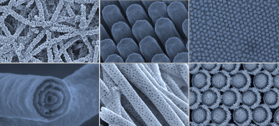
Fig. 1: Design of nanomaterials for energy, environmental and health applications [1]. C. Marichy, M. Bechelany, N. Pinna, Advanced Materials, 2012, 24, 1017 [2]. T. X. H. Le, R. Esmilaire, M. Drobek, M. Bechelany, C. Vallicari, D. L. Nguyen, A. Julbe, S. Tingry, M. Cretin Journal of Materials Chemistry A, 2016, 4, 17686-17693 [3]. M. Weber, B. Koonkaew, S. Balme, I. Utke, F. Picaud, I. Iatsunskyi, E. Coy, P. Miele, M. Bechelany, ACS Appl. Mater. Interfaces, 2017, 9, 16669–16678 [4]. M. Weber, A. Julbe, A. Ayral, P. Miele, M. Bechelany, Chemistry of Materials, 2018, 30, 7368-7390 [5]. O. Graniel, M. Weber, S. Balme, P. Miele, M. Bechelany, Biosensors and Bioelectronics, 2018, 122, 147-159 [6]. S. Nagarajan, H. Belaid, C. Céline Pochat-Bohatier, C. Teyssier, I. Iatsunskyi, E. Coy, S. Balme, D. Cornu, P. Miele, N. S. Kalkura, V. Cavaillès, M. Bechelany, ACS Appl. Mater. Interfaces, 2017, 9, 33695-33706
Development of high efficiency compact recuperators for micro gas turbines Michel DELANAYE MITIS SA, Belgium The lecture will focus on the development of design and modelling of high efficiency counter flow heat exchangers currently used by MITIS as recuperators for small micro gas turbines. A recuperator is a gas/gas heat exchanger which recuperates the heat from one stream to preheat combustion air. For small gas turbine, the recuperator plays an important role to achieve a high cycle electric efficiency. Challenges are to obtain high efficiency, low pressure losses and to be able to sustain the very high temperatures (above 700°C) in a corrosive environment while maintaining the cost as low as possible. Compactness is important since it reduces the amount of costly material used to build the recuperator. The lecture will detail the design methodology based on advanced CFD 3D modelling developed by MITIS in conjunction with reduced order modelling to achieve optimized heat exchangers. Manufacturing aspects will also be highlighted.
Optical, molecular sensitive, imaging monitoring techniques and applications in the microchannel Matthias RADLE, Marcel NACHTMANN, Carsten HOPF Mannheim University of Applied Sciences, Germany
In-situ and in-operando magnetic resonance spectroscopy Jens ANDERS Institute of Smart Sensors, University of Stuttgart, Germany
The work is supported by the DFG through the priority program SPP1601 and grant AN 984/10. 1. Handwerker et al., ISSCC 2016 Digest of Technical Papers, p. 476-478
ACTPHAST – towards a Photonics Innovation Hub for the Digital Transformation of European Industry Peter DOYLE B-Phot (Brussels Photonics Team) Vrije Universiteit Brussel (VUB), Belgium There is a real sense of urgency for digital transformation of European industry as the relative contribution of industry to the EU economy is declining. The European economy has lost a third of its industrial base over the past 40 years. Industry 4.0 presents a real opportunity to turn the tide in Europe’s favour, with a particular focus on SMEs and entrepreneurship which harness Europe’s excellent scientific base. Innovation and digitization go hand-in-hand as fundamental drivers of future prosperity. At the heart of this digital revolution lies Photonics. Photonics – the science and technology of harnessing light - is everywhere around us now. Yet we are only at the beginning of what is possible. As a Key Digital Technology targeted by the EU, photonics is essential to the functioning of the new applications which are powering Industry 4.0 and which are needed to address our major societal challenges. The outcome of the new digitization paradigm Industry 4.0 for European industry – incorporating both the photonics and “photonics-enabled” end user industries - will depend on European companies, the vast majority of which are SMEs, being ready and capable of seizing the opportunities afforded by digitization through innovation with photonics, faster and better than their global competitors. Unfortunately for most companies, especially SMEs, they are faced with significant obstacles because they don’t have the in-house expertise in photonics, or easy access to cutting-edge photonics technologies, to properly explore the innovation potential for their products. This is where ACTPHAST comes in. The ACTPHAST model is unique in a European context in that it is set up to provide a single entry point into a fully integrated prototyping supply chain across the broad spectrum of photonics technology platforms. ACTPHAST makes this cutting-edge photonics technology and expertise available in a subsidized format to any European company – with a particular emphasis on SMEs – for the purposes of collaborating on photonics innovation projects which will have a substantial impact on the companies’ business growth in terms of new revenues and job creation.
Taming Fire at Microscale: Molecular Simulations and Devices for Microcombustion Alina A. ALEXEENKO School of Aeronautics and Astronautics, Purdue University, USA Combustion at the microscale is an attractive technology for mobile power generation with energy densities ~100 times higher than the current battery technology. Enabling microcombustion technology has been an elusive goal since 1990s. Conventional combustors cannot be scaled down directly due to fundamental limitations of length and time scales related to ignition time, thermal and viscous losses and radical quenching. New device concepts integrating microscale phenomena such as field-emission microplasma can significantly alter thermal and reaction processes for sustained microcombustion. The direct simulation Monte Carlo method allows to study combustion phenomena at the molecular level including state-to-state processes at conditions far from thermal equilibrium. The evolution of computational platforms and availability of highly scalable DSMC software open an opportunity for molecular simulations to enable improved microcombustion understanding, diagnostics and control. Such modeling is especially useful for combustion at high speeds and at the microscale due to nonequilibrium transport and chemistry. In this talk we review a framework for applying DSMC to model combustion at the molecular level and apply plasma and flow simulations for microcombustion devices. A modified DSMC chemical reaction framework is developed to ensure detailed balance and relaxation towards thermal equilibrium regardless of the internal energy relaxation rates. First, we consider a benchmark of H2–O2 premixed flame and compare with continuum modeling and experimental data. The DSMC simulations based on the extended framework are then applied for other combustion examples. We also consider a novel microcombustion device concept based on field-emission dielectric barrier discharge. Field emission based microplasma actuators generate highly positive space charge that can be used to preheat, pump and mix reactants in microscale geometries and offer a promising solution to the problems associated with initiating and sustaining microcombustion. |


